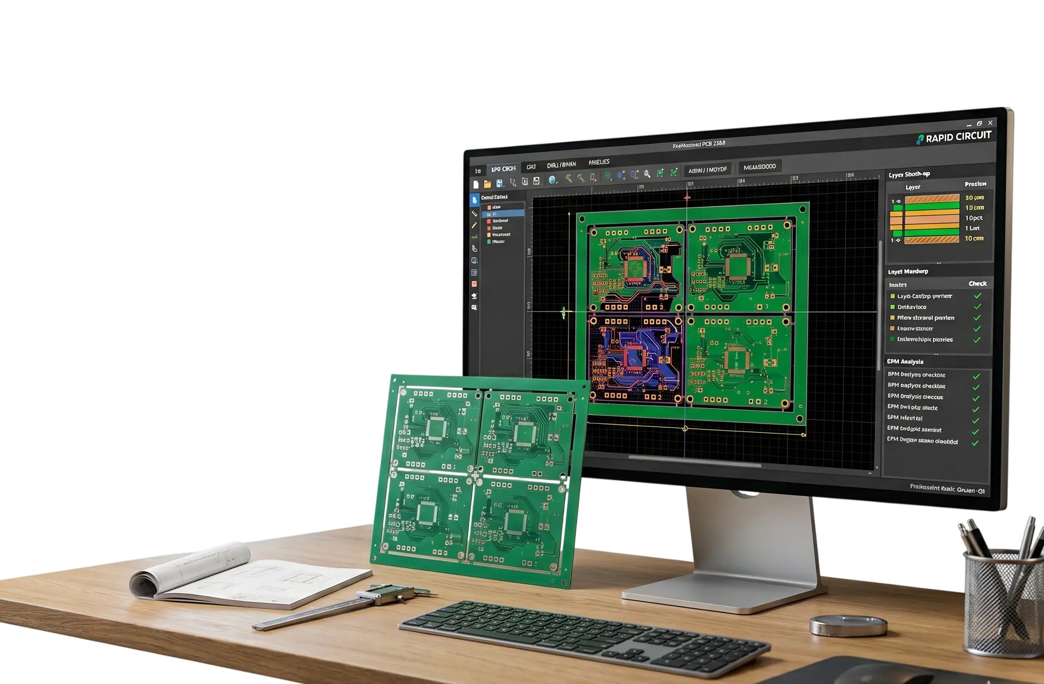
PCB CAM Work Service

PCB CAM Services | Front End Engineering

RapidCircuit offers end-to-end, high-precision PCB CAM services through a dedicated front-end engineering team, ensuring your printed circuit board designs are fully optimized for seamless manufacturing. Our Gerber data processing services include comprehensive checks, validations, and modifications to meet Design for Manufacturability (DFM), Design for Assembly (DFA), and Design for Test (DFT) standards.

With a modern and automated CAM infrastructure, Rapid Circuit supports a wide range of PCB technologies, including single-layer, multilayer, HDI, rigid-flex, RF/microwave, and high-speed digital boards.

We provide 24-hour turnaround CAM services along with overnight processing options for offshore clients. Serving companies across India, USA, UK, Germany, France, UAE, Saudi Arabia, and Australia, RapidCircuit delivers a strong time zone advantage. Our fast response capability helps reduce project delays, accelerate New Product Introduction (NPI), and stay ahead in competitive, time-sensitive markets.

RapidCircuit’s CAM outsourcing services are designed to lower operational costs and staffing overheads while improving production yield, minimizing fabrication errors, and speeding up time-to-market. Our expertise covers pre-production engineering activities such as Gerber merging, panelization, netlist comparison, drill and route optimization, stack-up validation, and impedance calculation.

We ensure complete CAM file integrity and compliance by checking for open circuits, short circuits, annular rings, solder mask clearance, silkscreen alignment, and other critical fabrication parameters. Additionally, we deliver manufacturing-ready output files, including Gerbers, NC drill files, pick-and-place data, and assembly drawings tailored to your fabricator’s specifications.

With extensive experience serving industries like automotive, medical devices, defense electronics, consumer products, and industrial automation, RapidCircuit stands as a trusted partner for high-reliability, production-ready PCB front-end engineering solutions. 

PCB CAM Service Capabilities

  • Full-fledged and dedicated CAM facility for the post-processing of Gerber data (Pre-Manufacturing)
  • 24/7 services to cater to the requirements of customers worldwide
  • State of the art Software/Hardware and Communication infrastructure
  • Netlist Analysis
  • Editing and Optimization
  • Rout and retain
  • Step and repeat with break-away tabs
  • Slots, Scoring, V-cuts, Routing
  • Tear dropping
  • Multiple circuit panelization
  • Creation of test coupons
  • Re-tool existing parts without disrupting current workload

PCB DRC/Analysis

  • Exhaustive list of design rule checks for all boards to avoid errors that may cause board scrap.
  • All features are thoroughly checked for violations before the board is panelized.
  • Some of the checks include:
  • A mismatch between Fabrication Drawing and Gerber.
  • The separation between segments.
  • Minimum track width.
  • Open trace / Hanging traces.
  • Power to ground short detection.
  • Annular ring verification.
  • Distance between holes to the copper segment.
  • Expose trace.

Editing/Single Image

  • Missing Hole, Extra Hole or Close Holes.
  • Touching Holes/Duplicate Holes.
  • Checking for the 2nd drill option.
  • Minimum spacing between two conductors.
  • Minimum Track width.
  • Minimum Annular ring.
  • Drill/rout to conductor spacing.
  • Sliver.
  • Thermal air gap/spoke width.
  • Drill to copper plane spacing.
  • Plane shear line width.
  • Mask annular ring for copper pad.
  • Expose trace.
  • Mask to copper spacing.
  • Legend width

PCB DRC/Analysis

  • Exhaustive list of design rule checks for all boards to avoid errors that may cause board scrap.
  • All features are thoroughly checked for violations before the board is panelized.
  • Some of the checks include:
  • A mismatch between Fabrication Drawing and Gerber.
  • The separation between segments.
  • Minimum track width.
  • Open trace / Hanging traces.
  • Power to ground short detection.
  • Annular ring verification.
  • Distance between holes to the copper segment.
  • Expose trace.

Cleanup

  • Draws to flash.
  • Pad Registration.
  • NFP Removal.
  • Redundant pad and line removal.
  • Line unification.
  • Contourization of self-intersecting polygons.
  • Sliver in acute angles.
  • SMD attributes.
  • Legend Detection.

Optimization

  • Power ground optimization.
  • Signal layer optimization.
  • Teardrop creation.
  • Solder mask optimization.
  • Legend overlap.
  • Copper balancing.
  • Etch compensation.

Special Product

  • Gold Finger.
  • Controlled Impedance.
  • Via-plug, Peelable mask, Carbon Ink.
  • Flip-flop panelization.
  • Flat pad.
  • Flex & Flex-Rigid.

Panelization

  • Step and repeat of board on large panel.
  • Venting pattern.
  • Tooling holes / Registration targets / Punch targets.
  • Coupons for controlled impedance jobs.
  • Compensation for lamination shrinkage.

Programming & Outputs

  • NC drill and rout programs.
  • After drill and before etching rout program for plated edges.
  • Second stage drill program.
  • Counter bore / Counter sink.
  • Panel with tab rout / Break-out pips.
  • Peck drill (G85).
  • Controlled depth rout.
  • Score program.
  • Tool path generation.
  • Cover layer and stiffener programs.

Scripting & Tooling Automation

  • Scripting – Enables customers to acquire the necessary scripts they need.
  • Hyper Tooling – A Java-based program developed for use in industrial environments.
  • Tooling – Delivered by a team of engineers providing complete tooling solutions.

PCB CAM , DFM Analysis Services

Our experienced and fully trained Sales Team is ready to answer any question related to our services and solutions.