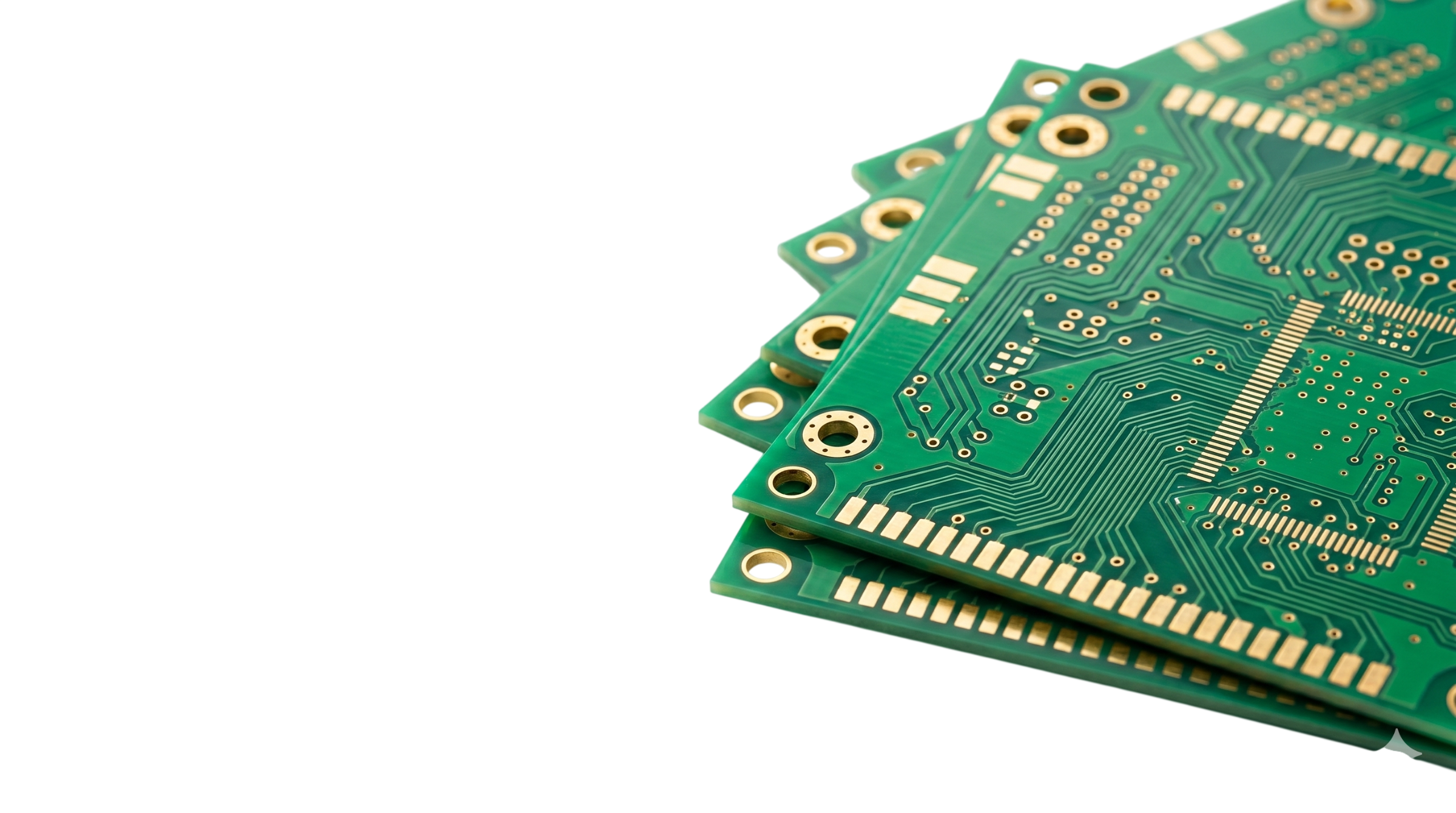
MULTILAYER PCB MANUFACTURING
High-Performance Multilayer PCB Manufacturing. Advanced. Reliable. High-Speed.
High-quality multilayer printed circuit boards engineered for superior signal integrity,
controlled impedance, and reliable thermal performance in telecommunications,
industrial automation, automotive systems, medical electronics, and high-speed
applications.
- High-Density PCB Design
- Superior Signal Integrity
- Controlled Impedance Support
- Reliable Multilayer Performance
Multilayer PCBs manufacturer
Advanced multilayer PCBs built for high-performance applications requiring complex circuitry and efficient signal management.
- High circuit density
- Enhanced performance
- Stable signal flow
Multilayer PCB Manufacturer in India
For complex electronic systems that demand high performance and compact design, choosing the right multilayer PCB manufacturer is critical. At RAPID CIRCUIT, we specialize in manufacturing precision multilayer PCBs for OEMs, telecom, automotive, and industrial applications, ensuring reliability from prototype to full-scale production.
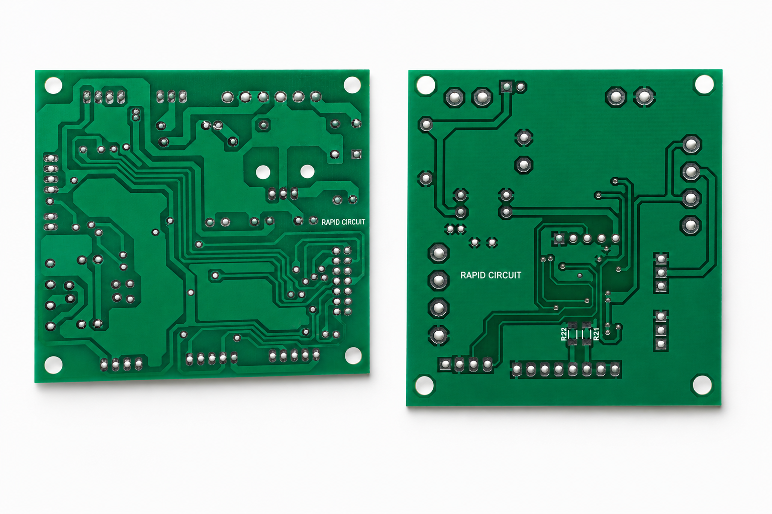
What is a Multilayer PCB?
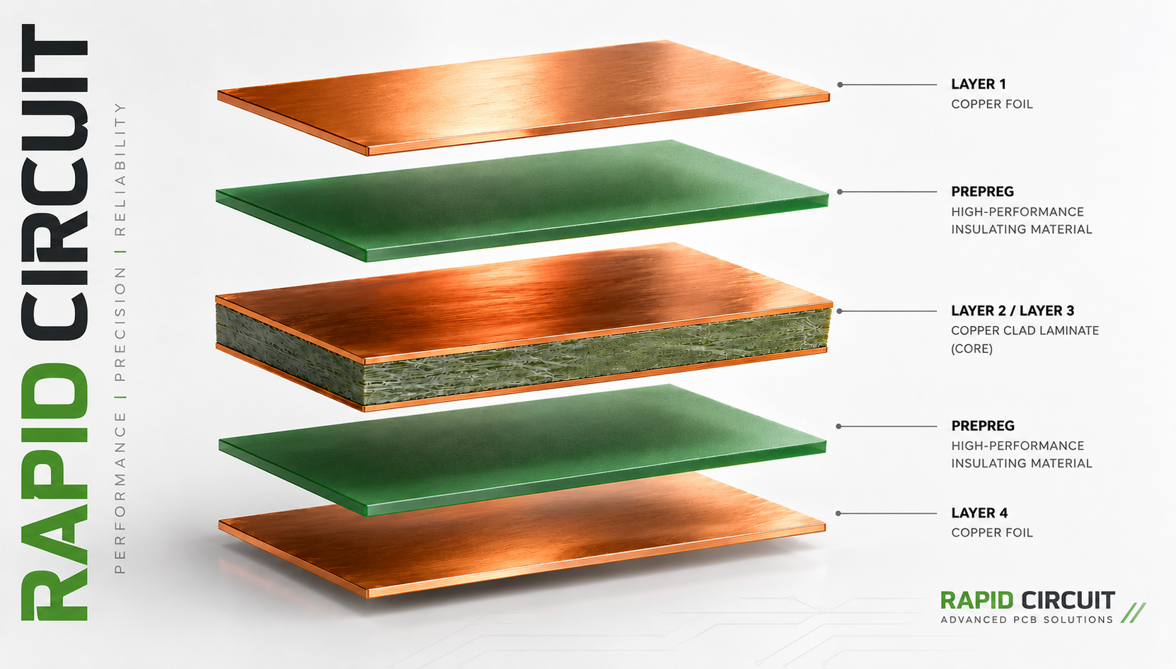
A multilayer PCB consists of four or more conductive copper layers stacked and bonded together with insulating material. These layers are interconnected using plated vias, enabling highly complex circuit routing within a compact footprint. Multilayer PCBs are essential for modern electronics requiring high speed, signal integrity, and space optimization.
Technical Specifications of Multilayer PCB
Material
• FR4 (standard)
• High TG FR4
• Rogers (high-frequency applications)
Board Thickness
• 0.8 mm to 3.2 mm
Copper Weight
• 0.5 oz to 3 oz
Surface Finish
• ENIG
• HASL (lead-free)
• Immersion Silver / Immersion Gold
Minimum Track / Spacing
• 4/4 mil (advanced capability)
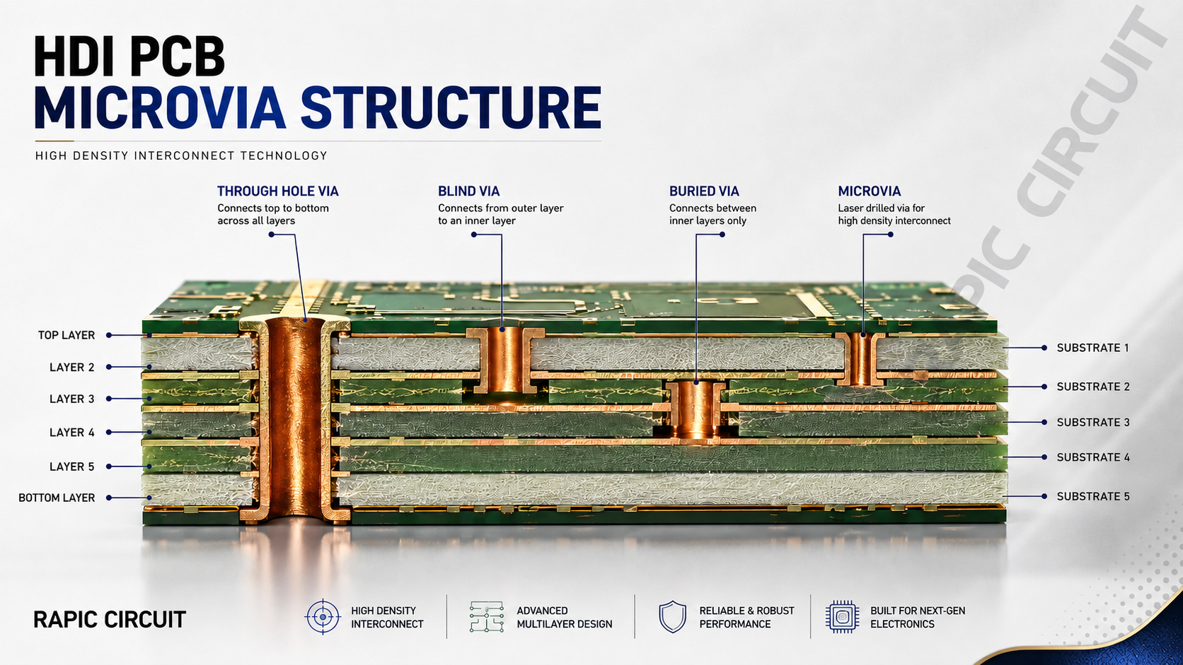
Minimum Hole Size
• 0.2 mm (microvias for HDI)
Need a high-performance multilayer PCB for your project?
Request a quote to get expert engineering support and optimized PCB solutions
Manufacturing Capabilities
• 4 to 16+ layer PCB fabrication
• Controlled impedance design
• HDI (High Density Interconnect) capability
• Precision layer alignment
• Multi-stage lamination
• Advanced CAM engineering
Features & Benefits
- High circuit density
- Improved signal integrity
- Reduced electromagnetic interference (EMI)
- Compact and lightweight design
- Suitable for high-speed applications
Applications & Industries
Multilayer PCBs are widely used in:
• Telecom infrastructure
• Automotive electronics (ADAS systems)
• Medical equipment
• Aerospace systems
• Industrial automation
• Consumer electronics
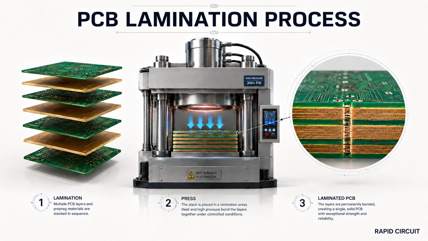
Multilayer PCB Manufacturing Process
Step 1 : Gerber File Submission
Design data is reviewed for multilayer stack-up feasibility
Step 2 : Multilayer PCB CAM Processing
Engineering checks include:
• Data Import & Gerber File Verification
• Registration & Layer Alignment
• Layer Stack-Up Verification
• Design Rule Check (DRC) for Multilayer PCB
• Drill Data Processing & Optimization
• Inner Layer Processing Checks
• Outer Layer Processing Checks
• Solder Mask & Silkscreen Verification
• Impedance & Signal Integrity Check
• Panelization (PCB Array Setup)
• Copper Balancing & Thieving
• Manufacturing File Generation
• Final CAM Review & Approval
Step 3: Production
• Material Preparation (FR4 Core & Prepreg Layer Setup)
• Inner Layer Imaging (PCB Circuit Pattern Transfer)
• Inner Layer Etching (Copper Trace Formation)
• Inner Layer Inspection – AOI (Automated Optical Inspection)
• Layer Stack-Up & Lamination (Multilayer PCB Bonding Process)
• PCB Drilling Process
• Hole Metallization – Plated Through Hole (PTH) Process
• Outer Layer Imaging & Copper Plating (Circuit Build-Up)
• Outer Layer Etching (Final Copper Pattern Formation)
• Solder Mask Application
• Silkscreen Printing (Component Legend & Marking)
Step 4: Quality Control
• Electrical testing
• Impedance verification
Step 5: Delivery
Secure packaging with global logistics support
Why Choose RAPID CIRCUIT
Pricing & Cost Factors
Multilayer PCB cost depends on:
- Number of layers
- Material type (FR4 vs high-frequency)
- Complexity of stack-up
- Via technology (through-hole vs microvia)
- Quantity
- Surface finish
- Testing requirements
Higher layers increase cost but significantly improve performance.
Experience
Strong expertise in complex PCB manufacturing.
Capabilities
Advanced infrastructure for high-layer PCBs.
Certifications
Industry-standard quality assurance processes.
Global Support
Serving clients across India and international markets.
Lead Time / Turnaround
Work with RAPID CIRCUIT for reliable, high-precision multilayer PCB manufacturing
Contact us today to discuss your requirements.
• Prototype: 7–8 days
• Small batch: 8–12 days
• Bulk production: 12–20 days
Expedited production available.
Explore Our PCB Solutions
FAQ
What is a multilayer PCB used for?
It is used in complex electronic systems such as telecom equipment, medical devices, and automotive electronics.
How many layers can a PCB have?
Multilayer PCBs can range from 4 layers to 16 or more, depending on design complexity.
What is the cost of multilayer PCB manufacturing?
Costs depend on layer count, materials, complexity, and volume.
What is the difference between double layer and multilayer PCB?
Double layer PCBs have two conductive layers, while multilayer PCBs have four or more, enabling higher circuit density.
How long does fabrication take?
Prototype production typically takes 7–8 days, while bulk production may take up to 18
days.
What materials are used?
FR4 is standard, with high-frequency materials like Rogers used for advanced
applications.
Can I order prototype multilayer PCBs?
Yes, prototyping is available before mass production