PCB Reverse Engineering Services in India

PCB Reverse Engineering Services in India

When original design files are unavailable or outdated, a professional PCB reverse engineering service becomes essential. At RAPID CIRCUIT, we help businesses recreate, analyze, and optimize existing PCBs for manufacturing, repair, or product improvement. Our engineering-driven approach ensures accurate design recovery while maintaining performance, reliability, and manufacturability. 

What is PCB Reverse Engineering?

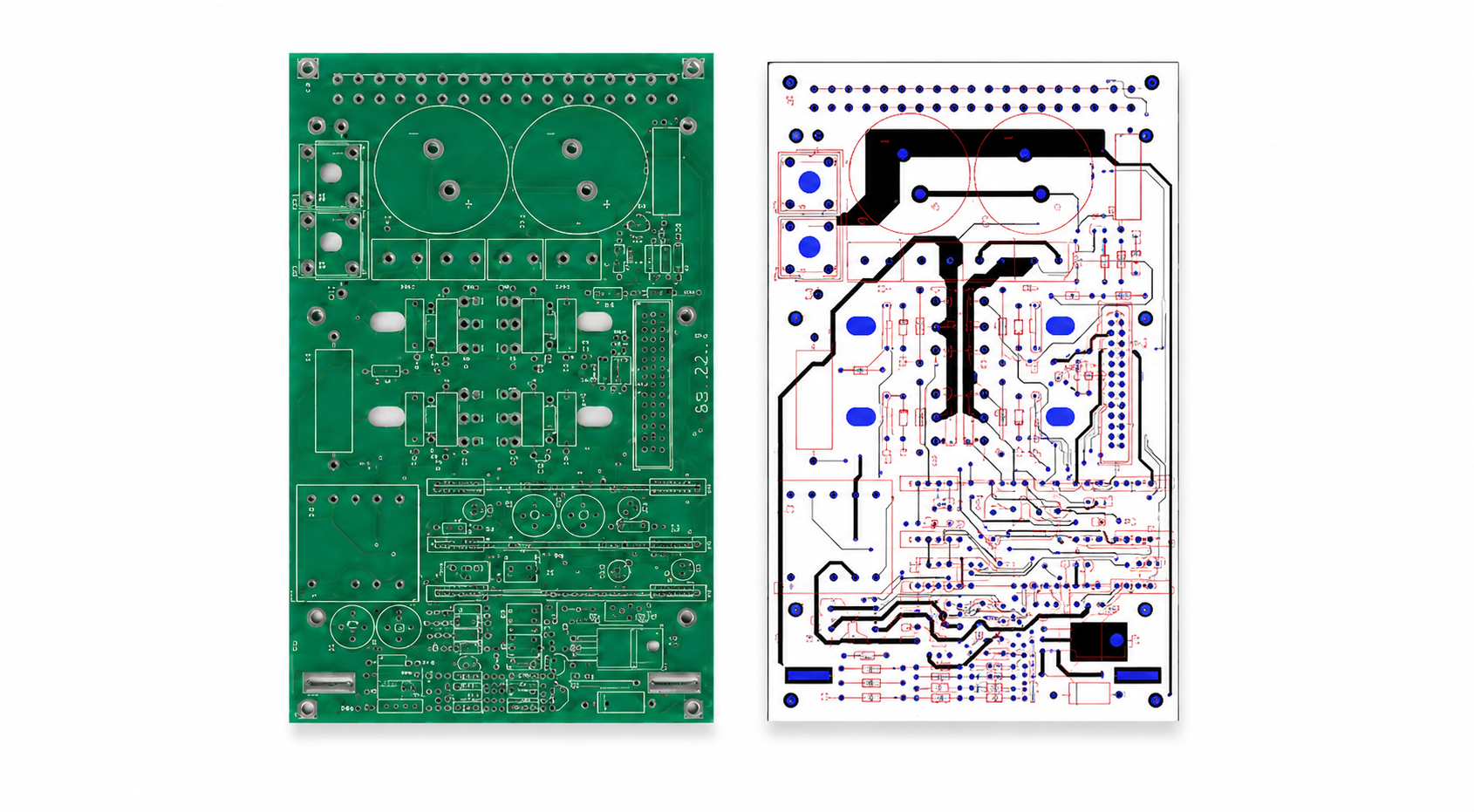
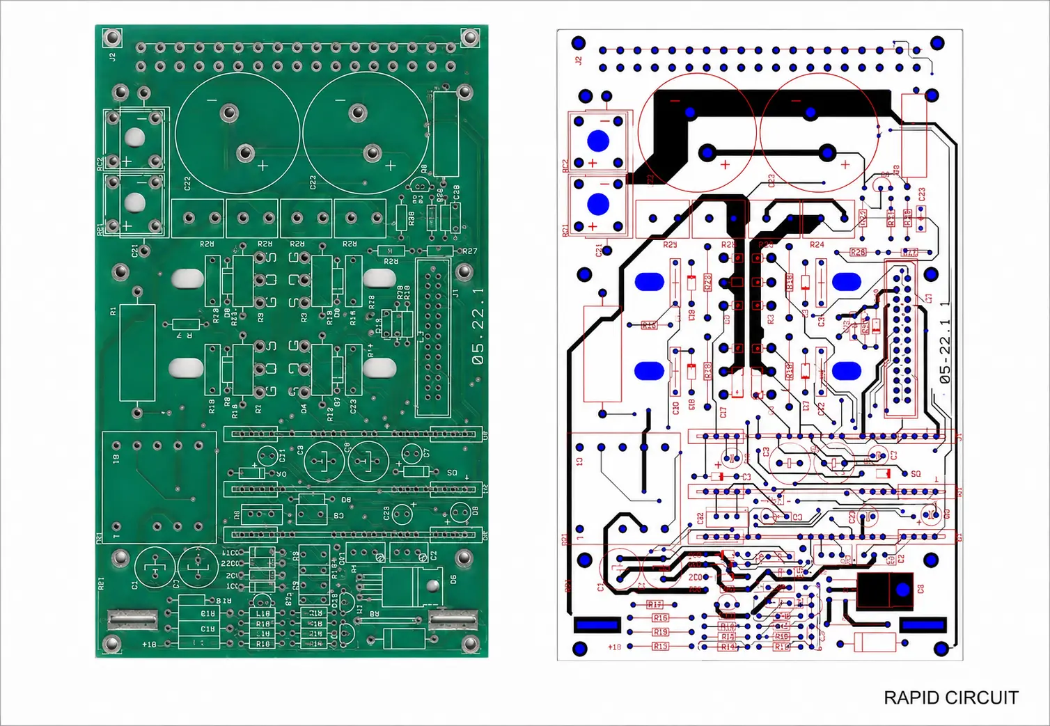
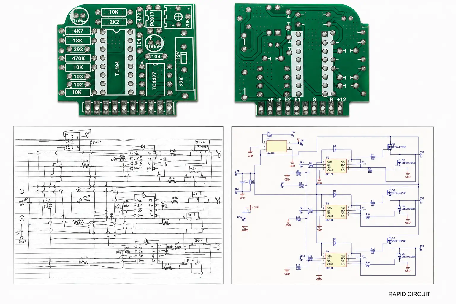
PCB reverse engineering is the process of analyzing an existing printed circuit board to recreate its design data, including schematic, layout, and manufacturing files. This service is commonly used when original design files are lost, obsolete, or need modification.


It allows companies to reproduce or improve existing PCBs without starting from
scratch.

Technical Specifications & Design Parameters

Material Analysis

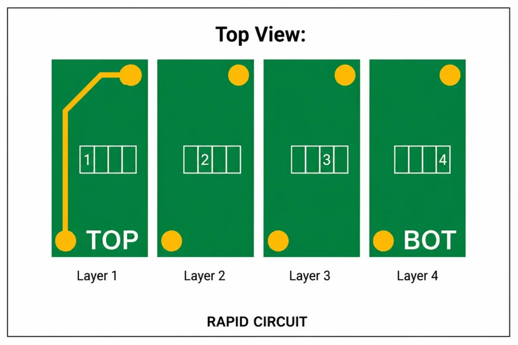
• FR4, CEM, metal core, and other substrates
• Layer stack-up identification

Board Thickness

• Measured and replicated accurately

Copper Weight

• Copper layer thickness verification

Surface Finish

• Identification of HASL, ENIG, OSP, etc.

Minimum Track / Spacing

• Extracted from existing design

Minimum Hole Size

• Drill size mapping and validation

Need to recreate or improve an existing PCB?

Get expert PCB reverse engineering support for your project.

PCB Reverse Engineering Capabilities

• Layer extraction and analysis
• Schematic reconstruction
• PCB layout recreation
• BOM generation
• Design optimization and redesign
• Gerber file creation
• Manufacturing-ready output

Features & Benefits

Applications & Industries

PCB reverse engineering is widely used in:
• Consumer electronics
• Automotive electronics
• Industrial equipment
• Telecom systems
• Medical devices
• Aerospace and defense

Reverse Engineering to Manufacturing Process

Step 1: PCB Analysis

Physical inspection and analysis of the PCB.

Step 2: Data Extraction

Layer-by-layer extraction of circuit information.

Step 3: Schematic Creation

Reconstruction of circuit diagram.

Step 4: PCB Layout Design

Recreating board layout with design optimization.

Step 5: CAM Processing

Preparing manufacturing-ready files.

Step 6: PCB Manufacturing

Fabrication using optimized data.

Step 7: Quality Testing

Electrical and functional testing.

Step 8: Delivery

Final product delivery with documentation.

Why Choose RAPID CIRCUIT

Pricing & Cost Factors

PCB reverse engineering cost depends on:

Experience

 Strong expertise in PCB design reverse engineering, and manufacturing.

Capabilities

Advanced tools for accurate PCB reconstruction.

Certifications

Strict quality and validation processes.

Global Support

Serving clients across India and worldwide.

Data Security

Confidential handling of client designs and IP.

Lead Time / Turnaround

Partner with RAPID CIRCUIT for reliable PCB reverse engineering services from analysis to production.

Contact us now to get started.

• Simple boards: 2–5 days
• Medium complexity: 5–10 days
• Complex multilayer: 10–20 days

Explore Our PCB Solutions

• pcb-layout-design-services
• pcb-cam-services
• pcb-manufacturer-india
• multilayer-pcb-manufacturer
• pcb-prototyping-services

FAQ

It is the process of recreating PCB design data from an existing board.

Yes, reverse engineering allows full design recovery.

It typically takes 2–20 days depending on complexity.

Automotive, industrial, telecom, medical, and electronics industries. 

Yes, with proper confidentiality and data protection practices. 

It depends on complexity, layers, and required output.  

Yes, redesign and optimization are part of the service. Â