PCB LAYOUT DESIGN SERVICES
Professional PCB Layout Design Services
Optimized. Reliable. Manufacturable.
Rapid Circuit provides professional PCB layout design services with optimized routing, signal integrity analysis, and DFM-compliant designs to ensure reliable performance, efficient manufacturability, and seamless integration for industrial, automotive, consumer, and high-speed electronic applications.
- Signal Integrity Optimization
- Precision PCB Routing
- DFM-Compliant PCB Design
- High-Reliability Layouts
PCB Layout Design Services in India
If you need a reliable partner to convert your circuit concepts into production-ready boards, choosing the right PCB layout design services provider is critical. At RAPID CIRCUIT, we offer end-to-end PCB design solutions, ensuring optimized layouts for performance, manufacturability, and cost efficiency—ideal for OEMs, startups, and industrial applications.
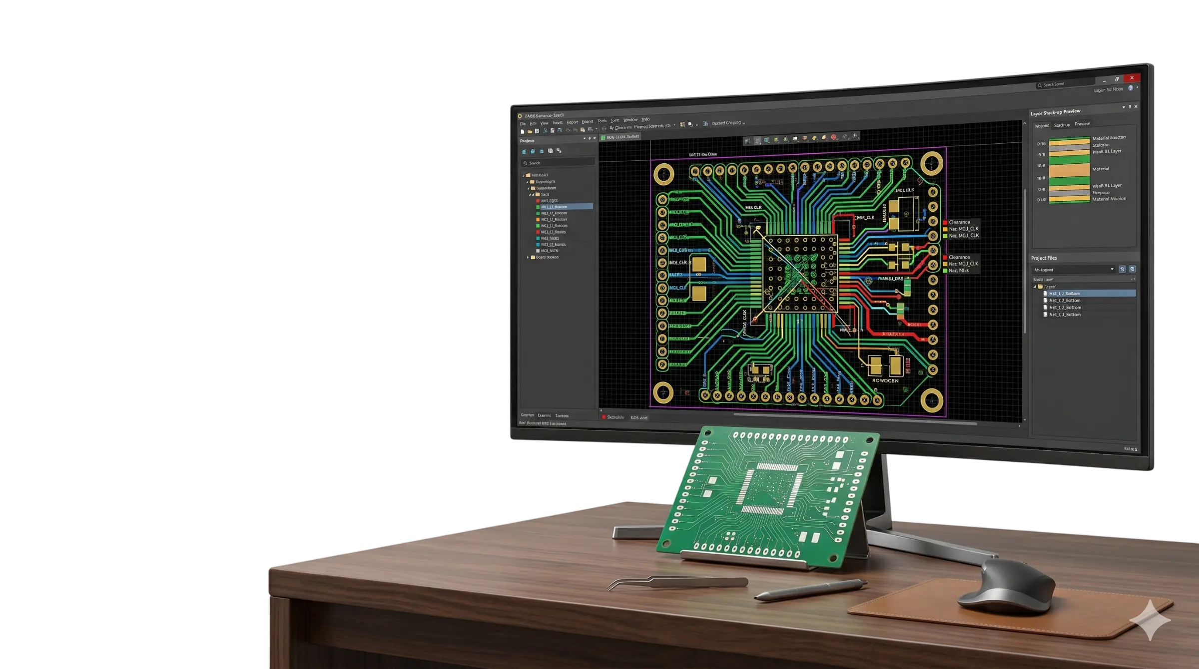
What is PCB Layout Design?
PCB layout design is the process of transforming a schematic diagram into a physical board layout by placing components and routing electrical connections. It ensures that the circuit performs reliably while meeting manufacturing and performance requirements.
A well-designed PCB layout directly impacts signal integrity, thermal performance, and product reliability.
Technical Design Capabilities
Design Tools
• KiCad for schematic capture and PCB design
Layer Capability
• Single layer
• Double layer
• Multilayer (up to 16+ layers)
Design Parameters
• Controlled impedance routing
• High speed signal routing and design
• EMI/EMC optimization
• Thermal management
Design Standards
• IPC standards compliance
• DFM (Design for Manufacturing)
• DFT (Design for Testing)
Need expert PCB layout design for your project?
Get a fast quote and expert PCB design consultation.
Design Services
• Schematic to PCB layout conversion
• High-speed PCB design
• Multilayer PCB layout
• RF and power circuit design
• Design optimization for cost reduction
• Gerber file generation
Features & Benefits
- Optimized for manufacturing efficiency
- Reduced production errors
- Improved signal performance
- Faster time-to-market
- Cost-effective design solutions
- Scalable for prototype to production
Applications & Industries
PCB layout design services are used in:
• Consumer electronics
• Automotive systems
• Industrial automation
• Telecom equipment
• Medical devices
• Power electronics
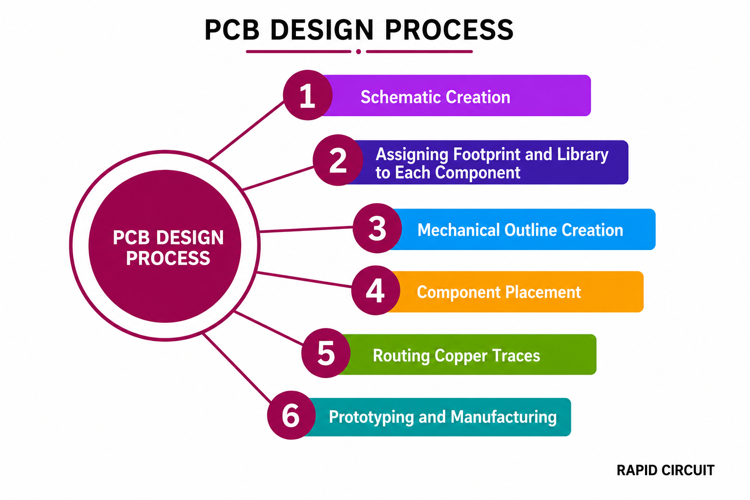
PCB Design Process
Step 1: Requirement Analysis
Understanding circuit requirements and specifications.
Step 2: Schematic Review
Validation of circuit design and Bill of Materials (BOM).
Step 3: Component Placement
Optimized placement for performance and manufacturability.
Step 4: Routing
Signal routing with impedance and EMI considerations.
Step 5: Design Verification
Electrical rule check (ERC) and design rule check (DRC).
Step 6: Output Generation
Gerber files and manufacturing documentation.
Why Choose RAPID CIRCUIT
Pricing & Cost Factors
PCB design cost depends on:
- Board complexity
- Number of layers
- Component density
- Design requirements (high-speed, RF, etc.)
- Turnaround time
Experience
Strong expertise in PCB design and manufacturing integration
Capabilities
Advanced design tools and engineering team.
Certifications
Compliance with industry standards.
Global Support
Serving clients across India and international markets.
Lead Time / Turnaround
Partner with RAPID CIRCUIT for reliable PCB layout design services from concept to production.
Contact us now to get started.
• Simple designs: 1–3 days
• Medium complexity: 3–7 days
• Complex multilayer: 7–14 days
Explore Our PCB Solutions
PCB Design Process Flow
Schematic Design
Draw complete circuit
Add net labels
Add protection circuits
Create hierarchical sheets
ERC Check
Floating pins check
Power conflicts
Missing connections
Net connectivity errors
Footprint Mapping
Assign PCB package
Verify pin pitch
Verify pad dimensions
Create custom footprints
PCB Stackup
Layer selection
Copper thickness
Controlled impedance
Material selection
Component Placement
Place connectors first
Signal flow optimization
EMI reduction
Thermal consideration
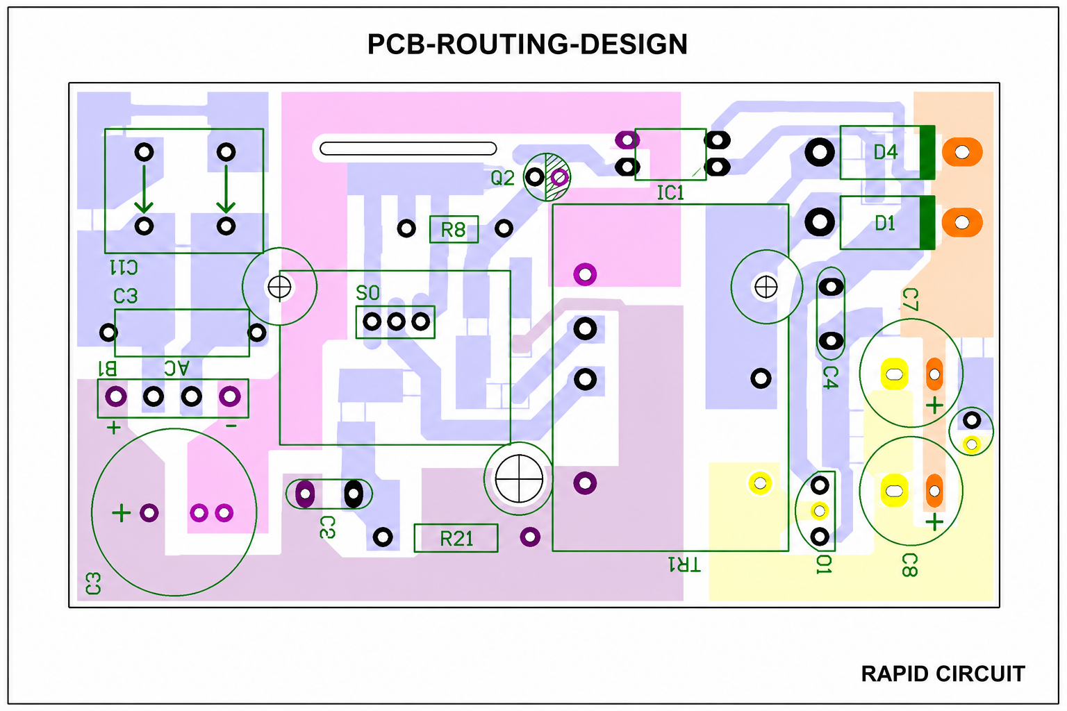
Signal Routing
Critical signals first
Clock routing
Length matching
Crosstalk reduction
DRC & Gerber
Clearance checks
Unrouted nets
Layer verification
Final inspection
Final Release
Documentation release
Manufacturing package
Gerber generation
Send to manufacturer
Design Flow
PCB Design Process Flow
Schematic Design
Draw complete circuit · Add net labels · Add protection circuits · Create hierarchical sheets
ERC Check
Floating pins check · Power conflicts · Missing connections · Net connectivity errors
Footprint Mapping
Assign PCB package · Verify pin pitch · Verify pad dimensions · Create custom footprints
PCB Stackup
Layer selection · Copper thickness · Controlled impedance · Material selection
Component Placement
Place connectors first · Signal flow optimization · EMI reduction · Thermal consideration
Signal Routing
Critical signals first · Clock routing · Length matching · Crosstalk reduction
DRC & Gerber
Clearance checks · Unrouted nets · Layer verification · Final inspection
Final Release
Documentation release · Manufacturing package · Gerber generation · Send to manufacturer
Design Flow
PCB Design Process Flow
Schematic Design
Draw complete circuit
Add net labels
Add protection circuits
Create hierarchical sheets
ERC Check
Floating pins check
Power conflicts
Missing connections
Net connectivity errors
Footprint Mapping
Assign PCB package
Verify pin pitch
Verify pad dimensions
Create custom footprints
PCB Stackup
Layer selection
Copper thickness
Controlled impedance
Material selection
Component Placement
Place connectors first
Signal flow optimization
EMI reduction
Thermal consideration
Signal Routing
Critical signals first
Clock routing
Length matching
Crosstalk reduction
DRC & Gerber
Clearance checks
Unrouted nets
Layer verification
Final inspection
Final Release
Documentation release
Manufacturing package
Gerber generation
Send to manufacturer
Design Flow
FAQ
What is PCB layout design?
It is the process of converting a schematic into a physical PCB layout with component placement and routing.
What is the cost of PCB design services?
Costs depend on complexity, layers, and design requirements.
How long does PCB design take?
Simple designs take 1–3 days, while complex designs may take up to 14 days.
What files are required for PCB layout design?
Schematic files, BOM, and design specifications are typically required.
What is the difference between schematic and PCB layout?
A schematic shows circuit connections, while PCB layout defines the physical board
design.
Can you design multilayer PCBs?
Yes, multilayer PCB design services are available.
Do you provide DFM support?
Yes, designs are optimized for manufacturing and testing.